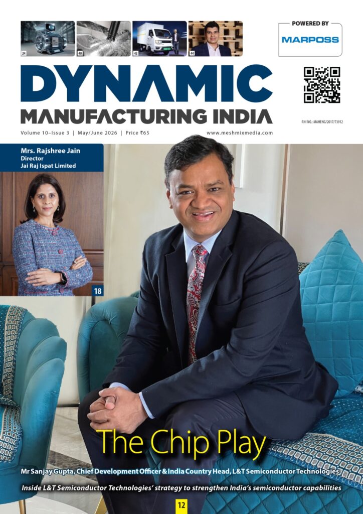
Inside L&T Semiconductor Technologies’ strategy to strengthen India’s semiconductor capabilities
India’s semiconductor ambitions are gaining unprecedented momentum as the country accelerates efforts to build a resilient electronics and semiconductor ecosystem. With strong policy backing, rising domestic demand, and increasing participation from global and Indian technology leaders, the semiconductor landscape is undergoing a transformational shift. At the forefront of this evolution is L&T Semiconductor Technologies (LTSCT), … The post Inside L&T Semiconductor Technologies’ strategy to strengthen India’s semiconductor capabilities appeared first on Machine Insider.
 machineryasia
India’s semiconductor ambitions are gaining unprecedented momentum as the country accelerates efforts to build a resilient electronics and semiconductor ecosystem. With strong policy backing, rising domestic demand, and increasing participation from global and Indian technology leaders, the semiconductor landscape is undergoing a transformational shift.
At the forefront of this evolution is L&T Semiconductor Technologies (LTSCT), a wholly owned subsidiary of Larsen & Toubro, focused on delivering high-performance semiconductor solutions for industries such as automotive, industrial, mobility, and advanced electronics. Leveraging L&T’s engineering heritage and deep expertise in complex systems, LTSCT aims to play a strategic role in strengthening India’s position in the global semiconductor value chain.
In this cover story, Sanjay Gupta, Chief Development Officer & India Country Head, L&T Semiconductor Technologies, shares insights into the company’s technology roadmap, the opportunities in India’s semiconductor design ecosystem, and how LTSCT plans to contribute to the nation’s vision of becoming a global semiconductor hub.

India’s semiconductor push has real momentum now — ₹76,000 crore committed, 10 fabs approved, Micron operational. What makes this moment different from previous attempts?
India’s semiconductor ambitions have reached an inflection point. The India Semiconductor Mission, with its ₹76,000 crore outlay and now ISM 2.0 in the 2026-27 Budget, has created a policy framework that’s genuinely transformational. What we’re seeing is a coordinated push across the entire value chain — from design to manufacturing to packaging.
The broader industry vision is about building strategic autonomy while remaining globally integrated. India currently imports $25-30 billion worth of semiconductors annually. The opportunity isn’t just about import substitution — it’s about positioning India as a critical node in the global supply chain, particularly for mature nodes (28nm-90nm) that power automotive, industrial, and consumer electronics.
What makes this moment different from previous attempts is the convergence of three factors: genuine policy commitment with fast-moving execution, a mature design ecosystem with 20,000+ engineers and 150+ indigenous startups, and strong market demand from India’s own electronics manufacturing growth. The alignment with India’s semiconductor mission is about contributing to this ecosystem-level development rather than any single company’s success.
With the semiconductor industry becoming critical to sectors such as automotive, industrial automation, and mobility, which application areas offer the fastest path to scale, and why?
The semiconductor industry is being reshaped by three mega-trends: electrification, intelligence, and connectivity. These converge most powerfully in automotive, industrial automation, and mobility — and that’s where the most compelling opportunities lie.
Automotive is undergoing the most dramatic transformation. An electric vehicle uses 2-3x more semiconductors than an ICE vehicle — roughly 1,400-1,500 chips per EV. The content is shifting from traditional microcontrollers to power semiconductors (IGBTs, SiC MOSFETs), sensors, and connectivity chips. India’s automotive sector, being the world’s fourth-largest, provides a massive domestic anchor market.
Industrial automation is equally compelling. Industry 4.0, predictive maintenance, smart manufacturing — all of this requires semiconductors for sensing, processing, and communication. The industrial semiconductor market is growing at 12-15% annually, driven by factory automation and IoT deployment.
Why these areas? First, they rely heavily on mature nodes (40nm-90nm) where India can compete effectively without needing the most cutting-edge (and capital-intensive) fabrication. Second, they have long product lifecycles — 10-15 years in automotive — which provides stability. Third, they’re less cyclical than consumer electronics. And fourth, India already has strong system-level expertise in these domains through its automotive and industrial manufacturing base.
India has 20,000+ design engineers and 125+ global design centers. How do we convert this talent advantage into indigenous IP and products?
The semiconductor ecosystem requires different capabilities at different stages. For India, the most relevant differentiators are in system-level integration, application engineering, and mature-node expertise.
System-level integration is where Indian engineering excellence shines. Understanding how semiconductors fit into larger systems — whether it’s an automotive powertrain, an industrial controller, or a consumer device — requires deep application knowledge. This is where decades of engineering heritage in complex systems becomes valuable.
Mature-node expertise is strategically important. While much attention goes to cutting-edge nodes (5nm, 3nm), the majority of chips used in automotive, industrial, and power applications are built on 28nm-90nm nodes. These nodes are less capital-intensive, have longer lifecycles, and face less geopolitical sensitivity. India’s manufacturing push appropriately includes significant focus on these nodes.
Compound semiconductors represent another differentiator. Silicon carbide (SiC) and gallium nitride (GaN) are critical for EVs, power electronics, and 5G. The upcoming SiC fab near Bhubaneswar (operational by 2028-29) positions India in this high-growth segment.
Advanced packaging is increasingly important as Moore’s Law slows. The Micron ATMP plant inaugurated in February 2026 and other OSAT facilities show India’s commitment to this segment. Packaging can deliver performance improvements without requiring the most advanced nodes.
The differentiator isn’t trying to replicate Taiwan or Korea’s model — it’s building a uniquely Indian approach that leverages existing strengths in engineering, design talent, and system integration.
What capabilities does India bring to the global semiconductor value chain that other regions don’t have?
The semiconductor ecosystem requires different capabilities at different stages. For India, the most relevant differentiators are in system-level integration, application engineering, and mature-node expertise.
System-level integration is where Indian engineering excellence shines. Understanding how semiconductors fit into larger systems — whether it’s an automotive powertrain, an industrial controller, or a consumer device — requires deep application knowledge. This is where decades of engineering heritage in complex systems becomes valuable.
Mature-node expertise is strategically important. While much attention goes to cutting-edge nodes (5nm, 3nm), the majority of chips used in automotive, industrial, and power applications are built on 28nm-90nm nodes. These nodes are less capital-intensive, have longer lifecycles, and face less geopolitical sensitivity. India’s manufacturing push appropriately includes significant focus on these nodes.
Compound semiconductors represent another differentiator. Silicon carbide (SiC) and gallium nitride (GaN) are critical for EVs, power electronics, and 5G. The upcoming SiC fab near Bhubaneswar (operational by 2028-29) positions India in this high-growth segment.
Advanced packaging is increasingly important as Moore’s Law slows. The Micron ATMP plant inaugurated in February 2026 and other OSAT facilities show India’s commitment to this segment. Packaging can deliver performance improvements without requiring the most advanced nodes.
The differentiator isn’t trying to replicate Taiwan or Korea’s model — it’s building a uniquely Indian approach that leverages existing strengths in engineering, design talent, and system integration.
The global semiconductor supply chain has undergone major disruptions in recent years. How do you see India’s role evolving in building a resilient and diversified semiconductor ecosystem?
The pandemic-era supply chain disruptions taught the industry a critical lesson: efficiency without resilience is fragility. The global semiconductor supply chain is now undergoing fundamental restructuring, and India has a significant role to play.
Geographic diversification is the first dimension. Companies and governments are actively reducing concentration risk. The U.S. CHIPS Act, Europe’s Chips Act, and India’s ISM all reflect this. India offers a compelling alternative — political stability, large domestic market, strong engineering base, and government commitment.
Supply chain depth is the second dimension. A resilient ecosystem needs more than just fabs — it needs equipment suppliers, materials providers, design tools, and packaging capabilities. India’s approach of supporting the full value chain (₹1.6 trillion in approved projects across fabs, ATMP, and display) reflects this understanding.
Strategic partnerships are the third dimension. No country can be self-sufficient in semiconductors. The goal is strategic autonomy, not autarky. India’s collaborations with the U.S., Japan, Netherlands, and others on technology transfer, equipment supply, and talent development are building these partnerships.
The “China Plus One” dynamic accelerates India’s opportunity. Many companies are diversifying manufacturing away from single-country dependence. India’s combination of market size, talent, and policy support makes it a natural beneficiary.
India’s role isn’t to replace existing hubs but to add redundancy and resilience to the global system — making the entire ecosystem more robust against future disruptions.
From your perspective, what are the key challenges India must address to accelerate its semiconductor ambitions—from design to manufacturing?
India’s semiconductor ambitions are real and achievable, but several challenges need focused attention:
Talent at scale: While we have 20,000+ design engineers, we need 50,000+ additional skilled professionals by 2030 — including fab operators, process engineers, equipment technicians, and materials scientists. This requires expanded university programs, industry-academia partnerships, and specialized training institutes. The C2S programme is a start, but scale needs to increase.
Infrastructure reliability: Semiconductor fabs require 24/7 reliable power, ultra-pure water, and vibration-free environments. India’s industrial infrastructure has improved dramatically, but fabs have zero-tolerance for disruptions. Dedicated infrastructure for semiconductor parks is essential.
Supply chain depth: India currently lacks indigenous capability in critical areas: semiconductor manufacturing equipment, specialty chemicals, high-purity materials, and EDA tools. Building this depth takes time — Taiwan and Korea took 20-30 years to develop their ecosystems. Patient capital and long-term commitment are required.
Capital intensity and patience: A leading-edge fab costs $15-20 billion and takes 3-5 years from announcement to production. Even mature-node fabs require $5-8 billion. Returns take 7-10 years to materialize. This requires investors and policymakers with long time horizons.
Regulatory agility: Semiconductor projects need fast environmental clearances, land acquisition, utility connections, and customs processing for equipment. The government’s new fast-track mechanisms are promising, but consistent execution across states is critical.
None of these challenges are insurmountable — but they do require sustained focus over multiple years, beyond election cycles and quarterly earnings.
India’s engineering heritage spans aerospace, defense, infrastructure. How does that systems expertise translate to semiconductor competitiveness?
The semiconductor industry is often viewed through a narrow lens — fabrication nodes, transistor counts, yield rates. But semiconductors are enablers, not end products. Their value is realized in the systems they power. This is where deep engineering heritage becomes a differentiator.
System understanding matters. Designing a chip for an automotive inverter requires understanding thermal management, power electronics, safety standards (ISO 26262), and real-world operating conditions. Companies with decades of experience building complex industrial and transportation systems bring this application knowledge inherently.
Integration capability is equally important. Semiconductors don’t work in isolation — they need to integrate with mechanical systems, software, connectivity, and user interfaces. Engineering organizations that have mastered multi-disciplinary integration can create more complete solutions.
Reliability and quality are non-negotiable in automotive and industrial applications. A consumer chip failure is an inconvenience; an automotive chip failure can be life-threatening. Engineering cultures built on safety-critical systems (nuclear, defense, railways, heavy industry) bring the rigor needed for these applications.
Customer proximity enables faster iteration and better solutions. Being close to automotive OEMs, industrial equipment manufacturers, and system integrators allows for co-development and rapid problem-solving.
The unique value proposition isn’t just making chips — it’s making chips that solve real industrial and automotive problems, backed by deep application expertise and system-level understanding.
Collaboration is essential in the semiconductor ecosystem. What partnerships — global players, academia, startups — matter most right now?
Semiconductors are the most collaborative industry in the world. No company — no country — does everything alone. The ecosystem spans design, IP, equipment, materials, fabrication, packaging, testing, and system integration. Collaboration isn’t optional; it’s existential.
Global technology partnerships are essential for technology access and market reach. This includes licensing IP from established players, partnering with equipment suppliers for fab setup, collaborating with foundries for manufacturing, and working with system companies for market access. India’s engagements with the U.S., Japan, Netherlands, and others reflect this reality.
Academia collaboration builds the talent pipeline and enables cutting-edge research. The Chips-to-Start-up programme’s 305 connected institutions is a strong foundation. But deeper collaboration is needed: joint research labs, curriculum co-development, faculty exchange, and student internships. Taiwan’s success was built on tight university-industry links.
Startup ecosystem drives innovation and agility. The 150+ Indian semiconductor startups are working on AI accelerators, analog chips, power semiconductors, RISC-V processors, and more. Larger players can collaborate through: pilot programs for startup technologies, mentorship and technical guidance, potential acquisition or investment, and providing market access.
Industry consortia enable pre-competitive collaboration on standards, shared infrastructure, and talent development. SEMI India, ISA, and other bodies play this role. Stronger participation and funding of these organizations amplifies their impact.
Open innovation models like RISC-V are particularly relevant for India. Open architectures reduce IP costs, enable customization, and build indigenous capability. India’s participation in RISC-V International and domestic RISC-V initiatives should accelerate.
The collaboration model should be: global partnerships for technology and markets, academia for talent and research, startups for innovation, and consortia for ecosystem development.
Fast forward to 2030: what does success look like for India’s semiconductor ecosystem? What’s the realistic ambition?
The semiconductor industry operates on long time horizons. A 3-5 year roadmap should focus on foundational milestones that enable longer-term success:
Year 1-2: Foundation
Manufacturing: First Indian fab begins production (Tata’s 50nm fab in Dholera expected 2026). OSAT facilities reach high-volume production.
Design: DLI-supported startups achieve 25+ tape-outs. At least 5-10 startups reach commercial production.
Talent: 10,000+ additional engineers trained through C2S and industry programs.
Supply chain: First indigenous equipment and materials suppliers qualify for fab integration.
Year 3-5: Scale
Manufacturing: 2-3 additional fabs operational (including SiC/GaN compound semiconductor facilities). India achieves 5-7% of global mature-node capacity.
Design: India-based design contributes 10-15% of global chip design work (up from current ~35-40% of design services). 3-5 Indian startups become significant global players.
Market: Domestic semiconductor consumption reaches $40-50 billion (from ~$25-30B today), with 20-25% sourced domestically.
Technology: Indigenous IP in power semiconductors, analog chips, and embedded processors. Participation in next-generation standards (6G, automotive Ethernet, industrial IoT).
Success metrics should include: number of tape-outs, fab utilization rates, export revenue, patents filed, talent trained, and domestic content in electronics manufacturing. The goal isn’t just capacity — it’s capability, competitiveness, and integration into global value chains.
The 3-5 year period should establish India as a credible, reliable semiconductor hub — not the largest, but strategically important and technologically competent.
Finally, what message would you like to share with India’s manufacturing and electronics industry about the role they can play in strengthening the country’s semiconductor ecosystem?
This is your moment. India’s semiconductor success isn’t just about semiconductor companies — it’s about the entire manufacturing and electronics ecosystem playing an active role.
Be a customer, not just an observer. The most powerful way to support India’s semiconductor ecosystem is to source from Indian suppliers. Work with Indian design companies. Qualify Indian-manufactured chips. Provide feedback and co-development opportunities. Domestic demand is the anchor that will make Indian semiconductors globally competitive.
Invest in the ecosystem. This doesn’t mean every company must build a fab. It means: investing in semiconductor startups, partnering with academia on talent development, participating in industry consortia, and advocating for supportive policies. Patient capital and long-term commitment are essential.
Build capabilities strategically. Identify where your company can contribute: design services, specialty manufacturing, equipment maintenance, materials supply, testing and validation. The ecosystem needs depth across all these areas.
Think globally from day one. Indian semiconductors must compete on quality, cost, and reliability — not just on being “Made in India.” Design for global markets. Certify to international standards. Build partnerships that provide market access.
Collaborate, don’t compete in isolation. The semiconductor industry rewards collaboration. Share pre-competitive research. Pool resources for talent development. Work together on policy advocacy. A rising tide lifts all boats.
The opportunity is generational. India has the policy support, the talent, the market, and the momentum. What’s needed now is sustained execution — from companies, from government, from academia. Ten years from now, we should be able to say: this was the decade India became a semiconductor power. Let’s make it happen — together.
The post Inside L&T Semiconductor Technologies’ strategy to strengthen India’s semiconductor capabilities appeared first on Machine Insider.